
Instrumentation
Ensure that all necessary training is complete prior to reserving instrumentation in ICAL. If you are unsure what training you need, please reach out to ical@sympa.montana.edu for assistance.
Current Instrumentation

Field Emission Scanning Electron Microscopes (FE-SEM)
Zeiss SUPRA 55VP and Zeiss Ultra 55
- Dual FE-SEMs provide high resolution imaging of varied engineered, biological and natural (geological)samples
- Ultra-high resolution at low accelerating voltage to allow nanometer scale imaging
- Backscatter (BSE) and secondary electron imaging (SEI) and InLens detector
- Energy Dispersive Spectrometry (EDS), large area and fast detector, for elemental analysis and mapping (Oxford Ultim detector)
- Electron back-scatted diffraction (EBSD) for in situ phase identification, crystal structure and crystallographic orientation determinations (Oxford Symmetry system)
- Variable pressure and high vacuum modes available
- Large volume sample analysis chamber
- Cathodoluminescence imaging with spectrometer for mapping trace element distribution (REEs and transition metals), residual strain, and spectroscopic determination of valence state with state-of-the-art Delmic system.
- Cryogenic stage for analysis of biological materials (e.g., biofilms)
- Tensile stage for real-time observation of materials under stress.
- Cryogenic stage for imaging biological tissues and ice
Manufacturers' websites & more information:
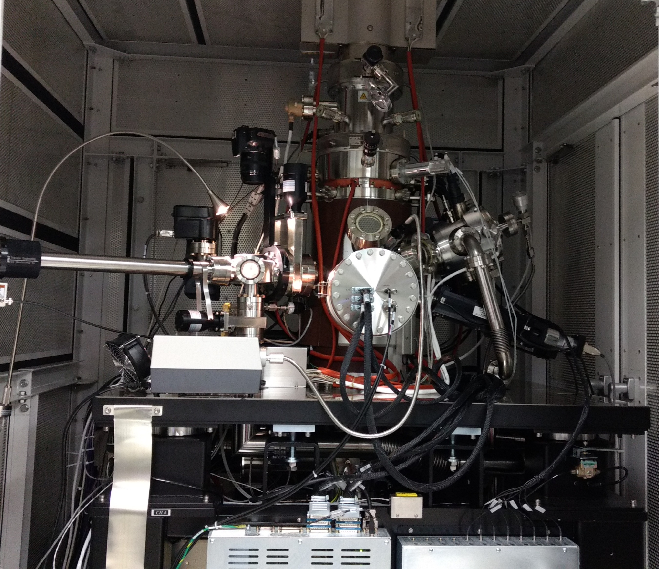
Scanning Auger Electron Nanoprobe (AES)
Physical Electronics 710
- Surface compositional analysis for all elements from Li (Z=3) and heavier of atomic monolayers (~1 nm)
- Quantitative analysis and mapping of surface components
- Sub-micron spatial analysis; enhanced lateral spatial resolution for elemental analysis (<8 nm with a 20kV, 1nA electron beam)
- Advanced charge compensation system allows for analysis of insulating materials
- Limited chemical (valence state) information
- Sputter depth profiling to characterize surficial stratigraphy (three dimensional analysis) using an Ar sputter gun
- EDS detector for “bulk” compositional analysis and mapping; allows for direct comparison of composition of “bulk” material and surficial composition measured by AES.
- EBSD detector for in situ phase identification, crystallographic orientation, and crystallographic preferred orientation and residual strain mapping
Manufacturer's website & more information:

Time-of-Flight Secondary Ion Mass Spectrometer (ToF-SIMS)
IONTOF GmbH, model IV
- For surface analysis of atomic monolayers on a 1-10 nm scale
- Mass resolution of around 5,000 m/∆m (~ 0.00x amu) and spatial resolution of ~ 1 µm
- Mass range of 0-10,000 amu
- Depth profiling of chemical stratigraphy of surface layers
- Trace element detection limits in ppm range
- Seamless positive and negative ion imaging modes
- Large sample loading area can accommodate up to 8-inch wafers
- Sub-micron imaging to map any mass number of interest
- Allows retrospective analysis with data cube giving full mass spectrum from every pixel
Manufacturer's website & more information:

X-ray Photoelectron Spectrometer (XPS)
Current Physical Electronics 5600 is not available as of 2022; a new instrument will be procured with NSF MRI funds 2026
- Elemental identification and quantification
- Chemical functional group identification and quantification
- Chemical state imaging
- Surface sensitivity
- Layer-by-layer depth profiling
- Minimal sample damage
- Analysis of insulating and conducting samples
- Data collection / stage automation
- Cold stage
Oxford Cypher Atomic Force Microscope (AFM)
Cypher AFM (with Blue Drive)
- Imaging of conducting and non-conducting surfaces
- Sub-nanometer resolution
- Imaging in air and liquid, allowing in-situ measurements and real time imaging of biological and chemical processes
- Contact and tapping modes of operation are available; ability to functionalize AFM tips to measure forces of chemical interactions
- AFM can be used to measure and localize many different forces including: adhesion strength, magnetic forces and mechanical properties
- True 3D imaging and measurements
- Magnetic, friction, chemical, and phase imaging
Manufacturer's website & more information:

Bruker D8 Advance Powder X-ray Diffractometer (XRD)
D8 Advance
- Features a unique D8 diffractometer family platform, perfect for all X-ray powder diffraction and scattering application
- Rapid phase identification based on X-ray diffraction patterns
- Non-destructive analysis of crystalline structures
- Large area X-ray detector produces high resolution XRD spectra; rapid data acquisition over a range of two-theta values
- Simple sample preparation (powder)
- Quantitative analysis of solid mixtures using Rietveld Method
- JADE software used for data reduction and interpretation; phase identification, Rietveld whole pattern fitting for quantitative analysis, unit cell refinement, determination of amorphous content, clay identification
- Standard Bragg-Brentano X-ray optics (convergent beam)
- Parallel beam X-ray optics for Grazing Incident Diffraction (GID; characterization of thin film phases) and X-ray Reflectometry (XRR; measurement of surface layer thickness, density and roughness)
Manufacturer's website & more information:
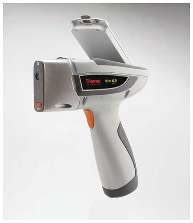
Portable X-ray Fluorescence (XRF)
Thermo Scientific Niton Gold XL3T Handheld X-ray Analyzer
- Bulk compositional analysis of solids and fluids
- Rapid, non-destructive data collection (~2 minutes)
- All elements from Mg and heavier, with PPM sensitivity for trace elements
- Detection limits of ppm
- Powdered samples are typically used, but other irregularly shaped solids (eg. art and archeology objects) and fluids can also be analyzed;
- Can be used on a platform in the lab or for in situ analysis in field settings.
- Routinely used to analyze rocks/soils; metals; ceramics; screening for toxic metals (Pb, As, Se, Cr, etc); forensic studies (e.g., archeological and art artefacts)
Manufacturer's website & more information:
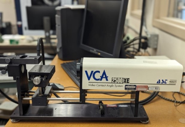
Video Contact Angle System
VCA 3500XE - ASC Products
- Provides contact angle measurement
- Determines surface energy
- Hydrophilicity/hydrophobicity of surfaces
- Gives information on surface cleanliness, roughness, etc.
Manufacturer's website:
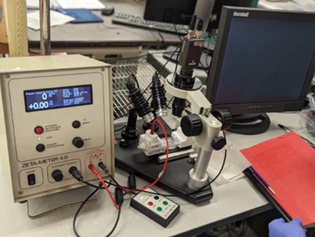
Zeta Potential Meter
Zeta-meter 4.0
- Provides indirect measure of the net charge on a nanoparticle
- Zeta potential values are determined via electrophoretic mobility measurements
- Obtains zeta potential values of nanoparticles in aqueous solution
- Gives criteria for the tendency of particles to flocculate (aggregate)
Manufacturer's website:
Epifluorescence Optical Microscope
OLYMPUS BX-61 (Not Available as of 2020)
- Precision objectives including air, oil and water immersion objectives
- Suite of reflected (fluorescent) filters (DAPI, FITC/CY2, TRITC/CY3, triple band and RBF)
- Significantly reduced autofluorescence and signal-to-noise ratio
- DIC imaging (10x, 20x, 40x, 60x)
- Digital camera imaging for still and time-lapse observations
More information:

Pella Carbon Coater for SEM sample prep
108 Carbon Coater
- High quality desktop vacuum coating systems
- 108 series sputter coaters for standard SEM and EDS sample coating
- Its dedicated thickness measurement system offers tight controls to create the desired coating thickness
- Better and more uniform coating on topographic samples
- Easy to use
More information:
Metal Coaters for SEM sample prep
- For sputter coating samples for SEM prep with metal conductive layer
- Two coaters: Dual source and dedicated source with interchangeable metal targets
- Dual source coater can provide alternating metal layers
- Adjustable current and time settings to give controlled layer thicknesses of 10-20 nm
- Available targets are iridium, gold, silver, platinum, and gold palladium to different applications
Manufacturer's website:
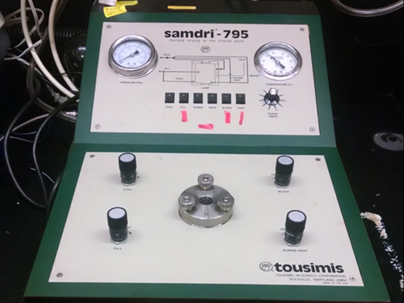
Critical Point Dryer (CPD)
- Alternative to air drying for vacuum samples
- Reduces imaging artifacts
- Uses liquid CO2
More information: