
Atomic Force Microscope
Cypher S and VEECO MultiMode V/Dimension 3100
Atomic force microscopy (AFM) is a powerful technique that allows imaging of non-conducting and conducting surfaces down to the sub-nanometer level without additional sample preparation. The AFM consists of a sharp tip (10–20 nm diameter) attached to a stiff cantilever. The tip is brought close to the sample surface, which is scanned beneath the tip. Interactions with the surface causes the tip to move up or down, and this tiny movement is measured using the displacement of a laser beam spot reflected off the back of the cantilever and collected by a photodiode.
The AFM is primarily run in one of two basic modes; contact and tapping. In contact mode the AFM tip is in continuous contact with the surface, whereas in tapping mode (also called intermittent contact mode) the AFM cantilever is oscillated near the sample surface, causing intermittent contact of the tip with the surface. This intermittent contact helps reduce shear forces associated with movement of the tip across the sample surface. Most AFM imaging is performed in the tapping mode, while contact mode AFM is only used for specific applications such as force curve measurements.
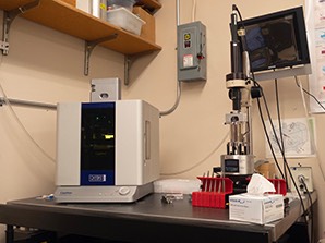
Two AFM instruments are available for users in ICAL, including a Cypher S instrument and a VEECO MultiMode V/Dimension 3100 instrument.
Cypher S: In addition to low-noise, atomic-scale topographic imaging capabilities, the Cypher S AFM provides a myriad of characterization techniques that can be performed in a range of environments. Both quasi-static and viscoelastic material properties can measured via fast force mapping and contact resonance imaging, respectively. Electromechanical coupling underlying the behavior of piezoelectric, ferroelectric, and certain biological materials can be measured using piezoresponse force microscopy. Kelvin probe force microscopy enables surface potential measurements based on differences in work function and voltage offsets while electrostatic force microscopy provides maps of force gradients generated by electrostatic charges. Conductive mapping techniques measure current through the AFM tip as a function of an applied sample bias and can be combined with fast force mapping to overlay sample conductivity onto maps of material modulus. The breakdown voltage of dielectric thin films can be characterized using a recently developed nanoscale time-dependent dielectric breakdown technique. Scanning microwave impedance microscopy maps variations in local capacitance and resistance, allowing users to see photo-current on ‘floating’ materials, or photovoltaic materials not built into a device. Fluid and electrochemistry cells are also available, broadly expanding the range of environments in which certain measurements can be performed. This instrument can run samples up to 15 mm in diameter and 7 mm thick. The maximum scan area is 30 μm×30 μm and maximum height scan is 5 μm.
VEECO MultiMode V/Dimension 3100: This instrument can run samples up to 15 mm in diameter and 7 mm thick. The maximum scan area is 10 μm×10 μm and maximum height scan is 2.5 μm.
In summary, the major advantages of AFM are:
- Imaging of conducting and non-conducting surfaces
- Sub-nanometer resolution
- Imaging in air and liquid, allowing in-situ measurements and real-time imaging of biological and chemical processes
- Can be used to measure and localize many different forces including adhesion strength, magnetic forces and mechanical properties
- True 3D imaging and measurements
- Capable of magnetic, friction, chemical, and phase imaging