
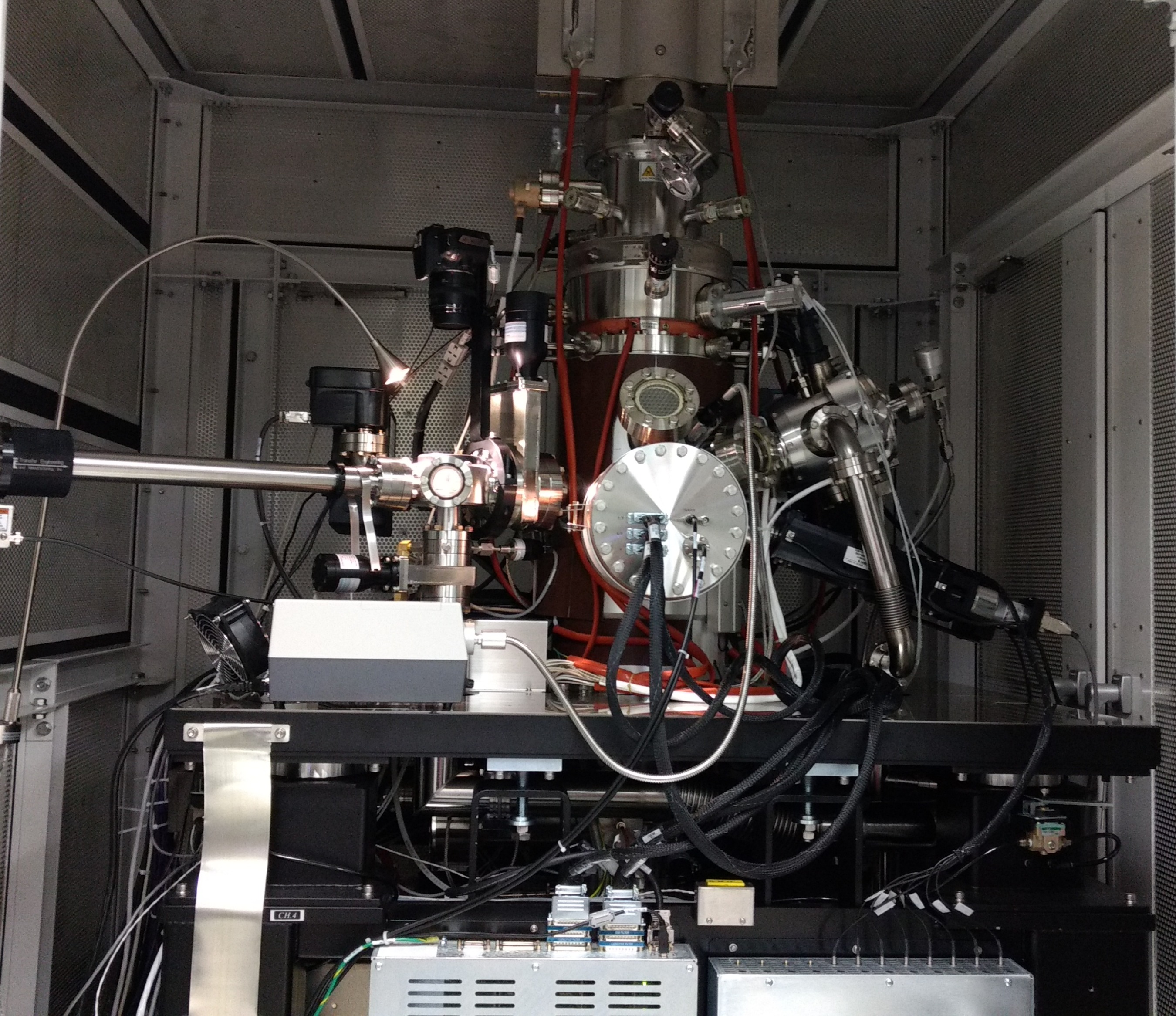
Scanning Auger Electron Nanoprobe
Physical Electronics 710
ICAL has recently acquired this Scanning Auger NanoProbe, which features EDS (energy-dispersive X-ray spectroscopy) and EBSD (electron backscattered diffraction) capabilities. In Auger spectroscopy (AES), like SEM, a highly focused and energetically well-defined electron beam is incident on the sample, whereupon electrons ejected from the sample are analyzed in terms of their kinetic energy and quantity. Some of these electrons are characteristic Auger electrons and, much like characteristic X-rays, are the fingerprint of the atoms from which they are emitted.
Because of the low kinetic energies of the ejected Auger electrons, their escape depth is limited to a few atomic layers.
Thus AES allows analysis of only the top atomic layers of the sample of interest. Therefore, Auger is a surface-sensitive technique (~5 nm) that complements the bulk X-ray microanalysis (~3 μm) of EDS. To allow observation below the surface of the sample, the system is equipped with in situ Ar-ion etching capability for depth profiling of the sample as well as charge compensation for insulating samples. The system operates under ultrahigh vacuum conditions with rapid sample introduction facilities. A secondary electron detector on this system allows high-resolution imaging, as previously described. Excepting hydrogen and helium, all elements can be detected.
In addition, the PHI 710 Scanning Electron Nanoprobe operated at ICAL is a one-of-a-kind instrument in the world. In addition to the Field Emission SEM (FESEM) and Auger Electron Spectroscopy (AES) capabilities, it is also equipped with an Energy Dispersive Spectrometer (EDS) and an Electron Backscattered Diffraction detector (EBSD). This allows real-time acquisition on the same region of interest (micron scale) of a) high resolution imaging (FESEM), spot analysis and elemental mapping (and depth profiling) of surface composition (AES), “bulk” elemental point analysis and mapping (EDS), phase identification based on diffraction patterns, crystallographic orientation (individual grains or grain maps, including residual stress maps; EBSD). The integration of these numerous data types provides a powerful tool to characterize physical and chemical properties of materials.
In summary, the advantages of AES are:
- Surface compositional analysis for all elements from Li (Z=3) and heavier of atomic monolayers (~1 nm)
- Quantitative analysis and mapping of surface components
- Sub-micron spatial analysis; enhanced lateral spatial resolution for elemental analysis (<8 nm with a 20kV, 1nA electron beam)
- Advanced charge compensation system allows for analysis of insulating materials
- Limited chemical (valence state) information
- Sputter depth profiling to characterize surficial stratigraphy (three dimensional analysis) using an Ar sputter gun
- EDS detector for “bulk” compositional analysis and mapping; allows for direct comparison of composition of “bulk” material and surficial composition measured by AES.
- EBSD detector for in situ phase identification, crystallographic orientation, and crystallographic preferred orientation and residual strain mapping
Further Reading About AES:
- D. Briggs and M. P. Seah, Practical Surface Analysis by Auger and X-ray Photoelectron Spectroscopy, John Wiley and Sons, New York, 1983.
- Powell, C.J. and Seah, M.P., 1990. Precision, accuracy, and uncertainty in quantitative surface analyses by Auger‐electron spectroscopy and x‐ray photoelectron spectroscopy. Journal of Vacuum Science & Technology A: Vacuum, Surfaces, and Films, 8(2), pp.735-763.
- Powell, C.J., Jablonski, A., Werner, W.S. and Smekal, W., 2005. Characterization of thin films on the nanometer scale by Auger electron spectroscopy and X-ray photoelectron spectroscopy. Applied Surface Science, 239(3-4), pp.470-480.
- Prutton, M., 2006, Scanning Auger Electron Microscopy, Wiley, 368 p.
Please refer to these tutorial websites for further information on instruments and methods described above: