
Instrumentation
Current Schedule
Atomic Force Microscope (AFM)
VEECO MultiMode V and Dimension 3100
- Imaging of conducting and non-conducting surfaces
- Sub-nanometer resolution
- Imaging in air and liquid, allowing in-situ measurements and real time imaging of biological and chemical processes
- AFM can be used to measure and localize many different forces including: adhesion strength, magnetic forces and mechanical properties
- True 3D imaging and measurements
- Magnetic, friction, chemical, and phase imaging
- MORE INFORMATION »
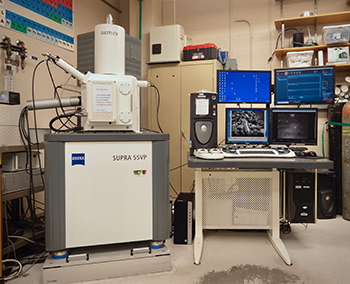
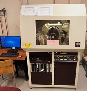
Field Emission Scanning Electron Microscope(FE SEM)
Zeiss SUPRA 55VP
- Ultra high resolution at low kV: 1.7nm @ 1.0kV, 4 nm @ 0.1kV
- Quantitative elemental analysis of the "bulk" material
- Fast elemental mapping and / or linescan of area of interest
- Topographical, compositional and other information
- Detection of small variations of trace element content
- Analysis and imaging of samples in their natural, hydrated state without the use of cryo
- Digital output
- Oil-free vacuum
- Large specimen capacity
- Rapid (10 minute turnaround) sample introduction
- MORE INFORMATION »
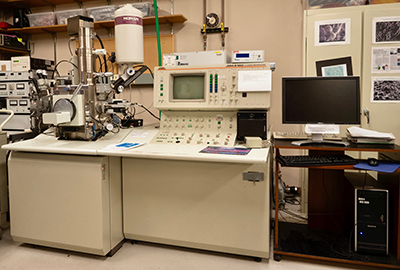
Scanning Electron Microscope (SEM)
JEOL JSM-6100
- Secondary Electron Imaging (SEI)
- Backscattered Electron Imaging (BEI)
- Cathodo-Luminescence detection and imaging (CL)
- Energy Dispersive x-ray Spectroscopy (X-Flash fast X-ray mapping detector)
- Cryo-preparation chamber with cold / hot stage
- High-resolution imaging
- Digital image capture
- Quantitative elemental analysis of the "bulk" material
- Fast elemental mapping and / or linescan of area of interest
- Topographical and density imaging
- Detection of small variations of trace element content
- Analysis and Imaging of samples in their natural, hydrated state
- MORE INFORMATION »
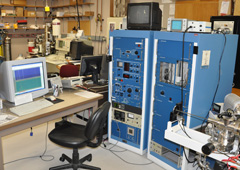
X-ray Photoelectron Spectrometer (XPS)
Physical Electronics 5600
- Elemental identification and quantification
- Chemical functional group identification and quantification
- Chemical state imaging
- Surface sensitivity
- Layer-by-layer depth profiling
- Minimal sample damage
- Analysis of insulating and conducting samples
- Data collection / stage automation
- Cold stage
- MORE INFORMATION »
X-ray Powder Diffraction Spectrometer (XRD)
Scintag X1 Diffraction System
- Rapid identification of materials
- Ease of sample preparation
- Computer-aided material identification
- Large library of known crystalline structures
- Multi-sample stage
- MORE INFORMATION »
Time-of-Flight Secondary Ion Mass Spectrometer (ToF-SIMS)
PHI TRIFT 1
- Chemical compound identification
- Elemental and chemical mapping
- Surface sensitivity
- Trace element sensitivity (ppm or ppb)
- Retrospective analysis
- Analysis of insulating and conducting samples
- Depth profiling
- Cold stage
- MORE INFORMATION »

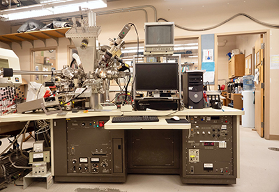
Scanning Auger Electron Nanoprobe (AUGER)
Physical Electronics 710
- Rapid sample introduction
- Low-Z elemental detection
- Quantitative analysis, mapping, linescan for AES and EDS
- Surface sensitivity of 1-5 nm
- Enhanced lateral spatial resolution for elemental analysis (<8 nm with a 20kV, 1nA electron beam )
- Limited chemical information
- Sputter depth profiling (three dimensional analysis)
- High resolution secondary electron imaging of analysis area
- MORE INFORMATION »
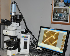
Epifluorescence Optical Microscope
OLYMPUS BX-61
- Precision objectives including air, oil and water immersion objectives
- Suite of reflected (fluorescent) filters (DAPI, FITC/CY2, TRITC/CY3, triple band and RBF)
- Significantly reduced autofluorescence and signal-to-noise ratio
- DIC imaging (10x, 20x, 40x, 60x)
- Digital camera imaging for still and time-lapse observations
- MORE INFORMATION »
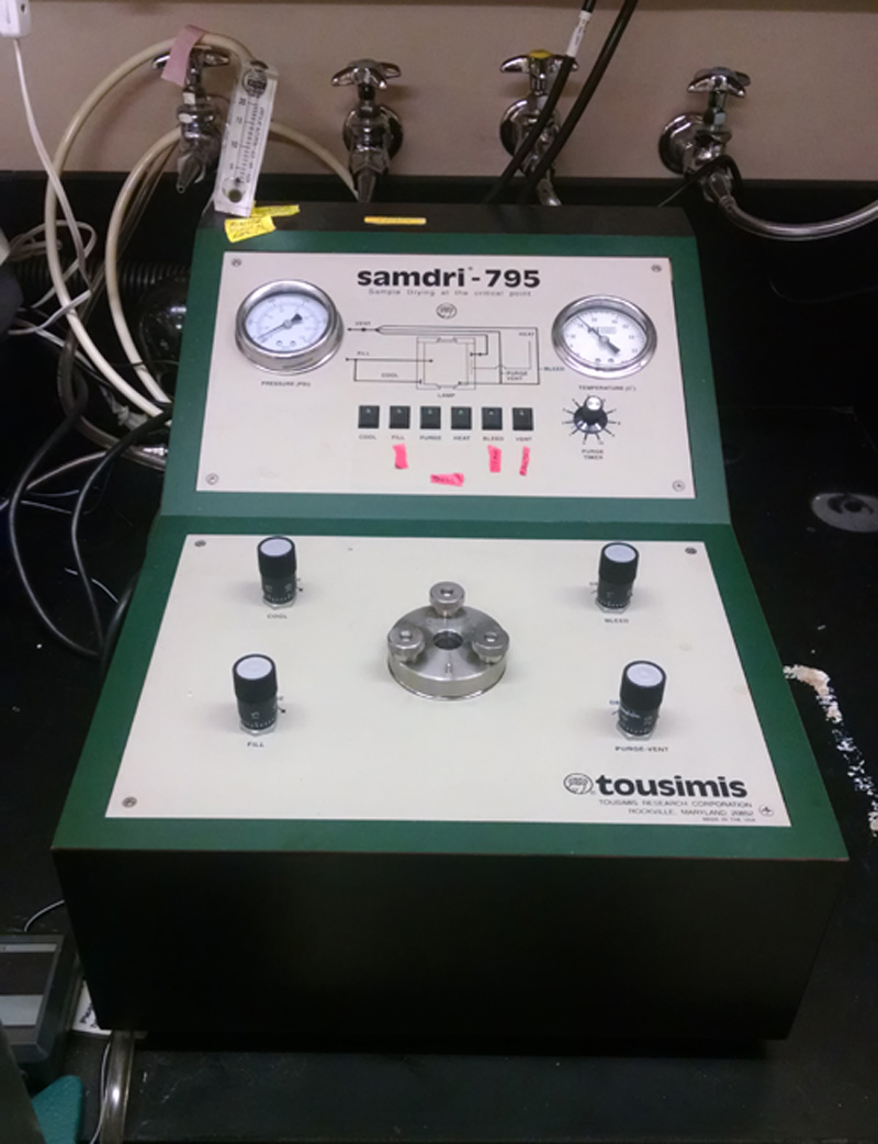
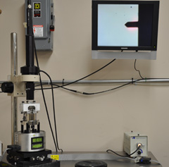
Critical Point Dryer (CPD)
Tousimis SAMDRI®-795
- Alternative to air drying for vacuum samples
- Reduces imaging artifacts
- Uses liquid CO2
- MORE INFORMATION »