
Field Emission Scanning Electron Microscope
Zeiss SUPRA 55VP
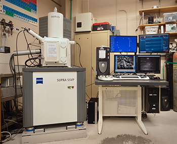
The FEM is a state-of-the-art electron microscope. The new field-emitter technology and advanced Gemini column allow for ultra-high resolution electron imaging, over x1,000,000 (>10nm at 1kV) for some samples. At such low voltages, non-conductive samples are easily imaged without coating.
The VP mode runs the sample chamber at high pressure (20-40Pa) which assisting in charge-compensation of the sample. This allows insulating samples to be analyzed and imaged without coating.
The EDS system detects X-rays emitted from the sample as a result of the high-energy electron beam penetrating into the sample. X-ray spectra can be collected and analyzed, yielding quantitative elemental information about the sample. A "standardless" routine is utilized, which yields an accuracy of 1-2% and sensitivities for some elements down to 0.1 weight percent. Linescans and x-ray maps can also be generated.
The Electron Backscattered Diffraction (EBSD) system utilizes a fluorescent screen
to capture the electrons diffracted from a crystalline sample. The diffraction pattern
is characteristic of the crystal structure and orientation of the sample region from
which is was generated. With the aid of very sophisticated software and multiple crystallographic
databases, crystal structures can be identified and oriented. For an expertly-polished
sample, mapping of orientations, stresses, morphologies, etc. are also possible.
In summary, the major advantages of FE SEM are:
- Ultra high resolution at low kV: 1.7nm @ 1.0kV, 4 nm @ 0.1kV
- Quantitative elemental analysis of the "bulk" material
- Fast elemental mapping and / or linescan of area of interest
- Topographical, compositional and other information
- Detection of small variations of trace element content
- Analysis and imaging of samples in their natural, hydrated state without the use of cryo
- Digital output
- Oil-free vacuum
- Large specimen capacity
- Rapid (10 minute turnaround) sample introduction